- 您现在的位置:买卖IC网 > Sheet目录1219 > HC5514XEVAL3 (Intersil)EVAL BOARD TI CODEC MOTHER BOARD
�� �
�
�Application� Note� 9871�
�7.� Connect� a� sine� wave� generator,� referenced� to� ground,� to�
�the� VRX� input.�
�8.� Set� the� generator� for� 1V� RMS� at� 1kHz.�
�9.� Connect� an� AC� voltmeter,� referenced� to� ground,� to� the�
�VTX� output.�
�Veri?cation�
�1.� 1.� The� 4-wire� to� 4-wire� transhybrid� balance� is� about� -24dB�
�as� calculated� in� Equation� 8.�
�Setup�
�1.� Connect� the� power� supplies� to� the� Evaluation� board.�
�2.� Set� V� BH� to� -48V,� V� BL� to� -24V� and� V� CC� to� +5V.�
�3.� Con?gure� the� SLIC� to� be� in� the� Test� Active� State�
�(C3� =� 0,� C2� =� 1,� C1� =� 1).�
�4.� Verify� that� the� POL/REV� pin� S4� (lower� right� hand� side� of�
�the� board)� is� in� either� the� 10ms� or� 20ms� position.�
�5.� Terminate� tip� and� ring� with� a� 600� ?� load.�
�dB� 4W� –� 4W� =� 20� log� -----------�
�V� TX�
�V� RX�
�(EQ.� 8)�
�6.� Connect� battery� backed� AC� (20Hz,� 90V� RMS� +V� BH� )�
�source� to� RING� GEN� INPUT� located� just� below� the� tip�
�and� ring� terminals� on� the� board.�
�Test� #9,� Line� Voltage� Measurement�
�Discussion�
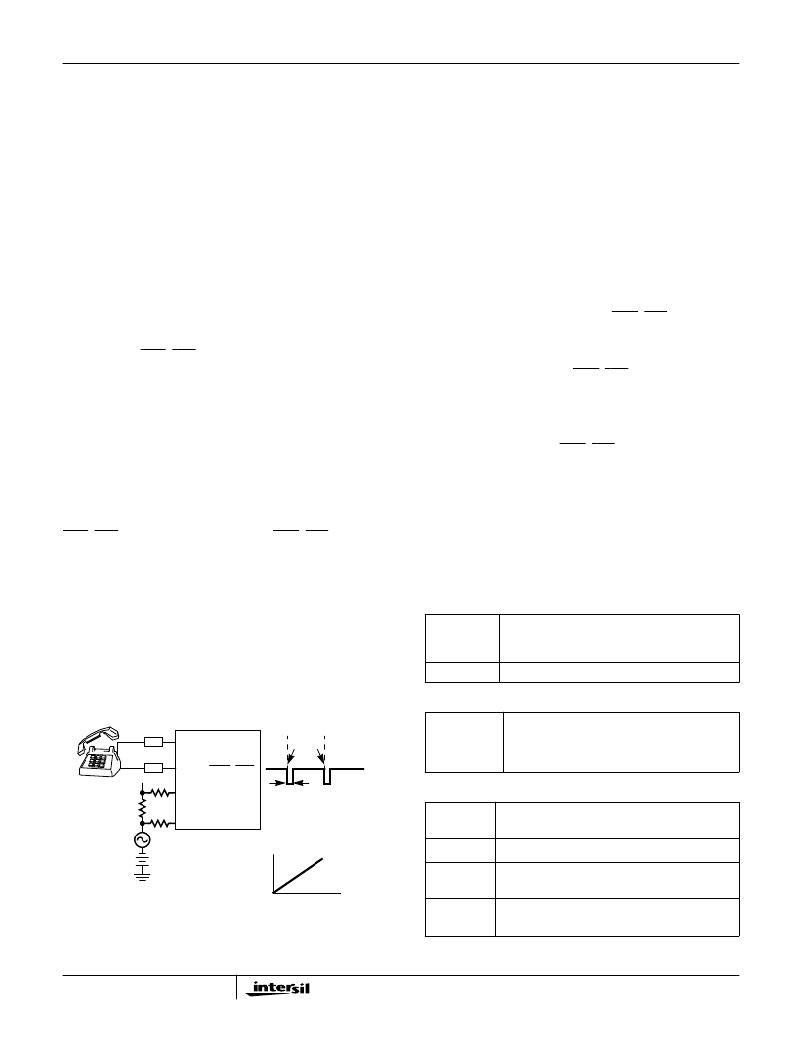
�A� few� of� the� SLICs� in� the� UniSLIC14� family� feature� Line�
�Voltage� Measurement� (LVM)� capability.� This� feature� provides�
�a� pulse� on� the� GKD_LVM� output� pin� that� is� proportional� to�
�the� loop� voltage.� Knowing� the� loop� voltage� and� thus� the� loop�
�length,� other� basic� cable� characteristics� such� as� attenuation�
�and� capacitance� can� be� inferred.� Decisions� can� be� made�
�about� gain� switching� in� the� CODEC� to� overcome� line� losses�
�and� veri?cation� of� the� 2-wire� circuit� integrity.�
�The� LVM� function� can� only� be� activated� in� the� off� hook�
�condition� in� either� the� forward� or� reverse� operating� states.�
�The� LVM� uses� the� ring� signal� supplied� to� the� SLIC� as� a� time�
�base� generator.� The� loop� resistance� is� determined� by�
�monitoring� the� pulse� width� of� the� output� signa� l� on� the�
�GKD_LVM� pin.� The� output� signal� on� the� GKD_LVM� pin� is� a�
�square� wave� for� which� the� average� duration� of� the� low� state�
�is� proportional� to� the� average� voltage� between� the� tip� and�
�ring� terminals.� The� loop� resistance� is� determined� by� the� tip�
�to� ring� voltage� and� the� constant� loop� current.� Reference�
�7.� Verify� that� pin� 2� of� the� PTG� jumper� (S8,� located� towards�
�the� middle� of� board� near� the� upper� right� hand� corner� of�
�the� SLIC)� is� ?oating.�
�8.� Monitor� the� output� signal� on� the� GKD_LVM� pin� with� a�
�scope.�
�Veri?cation�
�1.� The� output� signal� on� the� GKD_LVM� pin� is� a� square� wave�
�for� which� the� average� duration� of� the� low� state� is�
�proportional� to� the� average� voltage� between� the� tip� and�
�ring� terminals.�
�2.� Change� the� load� to� 1777� ?� load� and� notice� the� change� in�
�the� pulse� width� of� the� GKD_LVM� pulse.�
�3.� Notice� the� same� is� true� for� the� Test� Reversal� Active� State�
�(C3� =� 1,� C2� =� 1,� C1� =� 1).�
�Functional� Circuit� Component�
�Descriptions�
�A� brief� description� of� each� component� is� provided� below.�
�The� components� will� be� grouped� by� function� to� provide�
�further� insight� into� the� operation� of� the� HC5514X� board.�
�TABLE� 4.� TWO� WIRE� SIDE,� TIP� AND� RING�
�Figure� 6.�
�Although� the� logic� state� changes� to� the� Test� Active� State�
�when� performing� this� test,� the� SLIC� is� still� powered� up� in� the�
�active� state� (forward� or� reverse)� and� the� subscriber� is�
�RP1,� RP2�
�U2�
�Protection� Resistors� used� for� limiting� the� current�
�into� the� transient� voltage� suppressor� in� the� event� of�
�a� surge.�
�Secondary� Surge� Protection.�
�unaware� the� measurement� is� being� taken.�
�TABLE� 5.� POWER� SHARING�
�TIP�
�UniSLIC14�
�RING�
�GEN�
�FREQ�
�R13,� S9�
�R13� (R� PS� )� is� used� to� provide� off-chip� power�
�dissipation� to� prevent� the� SLIC� from� going� into�
�thermal� shutdown� in� short� loop� high� power�
�RING�
�DR�
�GKD_LVM�
�PULSE� WIDTH�
�PROPORTIONAL� TO�
�applications.�
�TABLE� 6.� PROGRAMMABLE� FEATURES� OF� THE� HC5514X�
�DT�
�LOOP� LENGTH�
�R1,� C7�
�R1� is� used� to� set� the� overhead� voltage.� C7� provides�
�filtering� for� the� DC� loop� and� Anti� Clipping� circuitry.�
�RING�
�GEN�
�LOOP� LENGTH�
�FIGURE� 6.� OPERATION� OF� THE� LINE� VOLTAGE�
�MEASUREMENT� CIRCUIT�
�7�
�C3�
�R4�
�R5�
�CDC� Provides� filtering� of� the� DC� loop.�
�RD� Resistor.� Used� to� set� the� offhook� detect�
�threshold.�
�ROH� Resistor.� Used� to� set� the� minimum� loop�
�current� with� maximum� overhead� voltage.�
�发布紧急采购,3分钟左右您将得到回复。
相关PDF资料
HC55185EVAL2
EVALUATION PLATFORM HC55185+T
HE1015
BOOT CIRCUIT BREAKER 1POLE CLEAR
HE1020
BOOT CIRCUIT BREAKER 2POLE CLEAR
HE1050
BOOT CIRCUIT BREAKER 3POLE CLEAR
HE1070
BOOT CIRCUIT BREAKER 3POLE CLEAR
HFW30R-1STE1
HFW30R-1STE1-FFC/FPC CONN
HFW30S-2STE1
HFW30S-2STE1-USING HFW-P5SL
HHG
FUSEHOLDER AUTO INLINE FOR ATC
相关代理商/技术参数
HC5515
制造商:INTERSIL 制造商全称:Intersil Corporation 功能描述:ITU CO/PABX SLIC with Low Power Standby
HC5515_06
制造商:INTERSIL 制造商全称:Intersil Corporation 功能描述:ITU CO/PABX SLIC with Low Power Standby
HC55150
制造商:INTERSIL 制造商全称:Intersil Corporation 功能描述:Low Power Universal SLIC Family
HC55150CB
制造商:Rochester Electronics LLC 功能描述:LOW PWR SLIC,POL REV/METERING,55DB BALANCE - Bulk
HC55150CBZ
功能描述:电信线路管理 IC LW PWR SLIC POLV/MTRING 55DB RoHS:否 制造商:STMicroelectronics 产品:PHY 接口类型:UART 电源电压-最大:18 V 电源电压-最小:8 V 电源电流:30 mA 最大工作温度:+ 85 C 最小工作温度:- 40 C 安装风格:SMD/SMT 封装 / 箱体:VFQFPN-48 封装:Tray
HC55150CM
制造商:Rochester Electronics LLC 功能描述:LOW PWR SLIC,POL REV/METERING,55DB BALANCE - Bulk
HC55150CMZ
功能描述:电信线路管理 IC LW PWR SLIC POLV/MTRING 55DB RoHS:否 制造商:STMicroelectronics 产品:PHY 接口类型:UART 电源电压-最大:18 V 电源电压-最小:8 V 电源电流:30 mA 最大工作温度:+ 85 C 最小工作温度:- 40 C 安装风格:SMD/SMT 封装 / 箱体:VFQFPN-48 封装:Tray
HC55151
制造商:INTERSIL 制造商全称:Intersil Corporation 功能描述:Low Power Universal SLIC Family